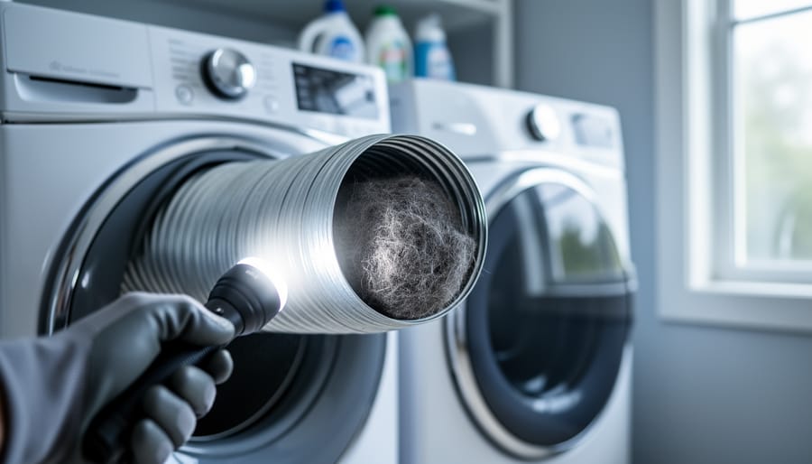
Check your dryer vent every three months for lint buildup by disconnecting the duct from the back of your dryer and visually inspecting it with a flashlight. If you notice longer drying times or your laundry room feels unusually warm, these are clear signs your vent needs attention. For comprehensive guidance on professional maintenance options, visit this site to explore expert cleaning services in your area.
Your dryer vent silently drains your wallet and the environment. A clogged vent forces your dryer to work up to 30% harder, transforming …

These Energy Upgrades Help You Sell Your House Fast (Even to Cash Buyers)
Focus your energy upgrade budget on visible improvements that reduce buyer concerns and lower running costs. If you’re considering Property Saviour or similar cash buyers, understand that while they prioritize speed over premium prices, strategic energy upgrades can still influence their offers and broaden your buyer pool.
Install LED lighting throughout your home for under £100—it’s the fastest upgrade that signals energy consciousness to viewers within seconds of walking through your door. Replace outdated thermostats with programmable models for £50-150, demonstrating …

Are Pellet Stoves Energy Efficient?
In an era where energy efficiency is not just a preference but a necessity, pellet stoves have emerged as a compelling alternative to conventional heating methods. The question “Are pellet stoves energy efficient?” is increasingly relevant. That’s expected as homeowners seek sustainable and cost-effective home heating solutions. Unlike a traditional wood stove, installing a pellet stove offers a unique combination of convenience, efficiency, and environmental friendliness.
Hence, they are an attractive option…

How to Heat a Swimming Pool for Free
Swimming pools offer a world of enjoyment, but the costs associated with heating them can be a real dampener. However, various ingenious ways help to tap into nature’s resources and warm your pool without breaking the bank.
This article will discuss several effective methods to heat your swimming pool using free and sustainable energy sources.
Embrace Solar Power
Harnessing the sun’s energy is a popular and eco-friendly method to heat your swimming pool. Solar pool heating systems, including a solar pool heater and liquid solar cover, use …
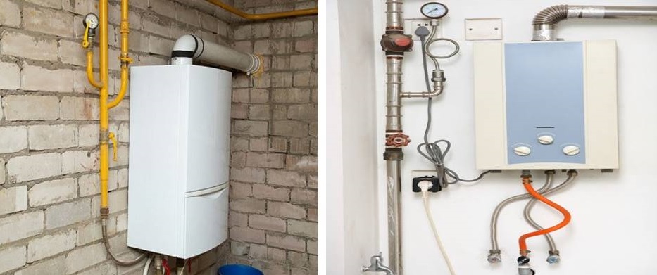
Boiler vs Water Heater: Understanding the Differences
When it comes to providing hot water for your home, you may have heard the terms “boiler” and “water heater” used interchangeably and think they have the same functions. While both devices are used to heat water, they have distinct differences in their construction, functions, and capabilities. In this article, we will explore the differences between a boiler and a water heater and help you choose the best option for your hot water needs.
The Difference Between a Boiler and a Water Heater?
Before we delve into the details, let’s define what a boiler and water heater are …

Saving Energy is a Lifestyle not a Diet
Saving energy is something that everyone should be aware of. If the gravity of the issue is not explained, people will be unable to make lifestyle adjustments and informed.
Energy-efficient decisions are necessary, especially in the modern times we are living in. Understanding why choices are important motivates and empowers people to make excellent decisions. This saves our planet from carbon and leaves money for other purposes after cutting down energy expenses.
…

Help with High Winter Heating Costs
The cost of heating throughout the winter months can be rather high. In reality, electricity and natural gas prices are around 12 percent more than a year earlier, while residential heating oil prices are up over 40%. The government has made a commitment to provide funding through the Low Income Home Energy Assistance Program to help low-income earners cover heating costs. This is particularly the case in cold-weather areas.
Calculating how much electricity your appliances and household electronics consume will help you figure out how much money you’re spending on them. To determine whether to invest in a more …

Start 2022 with a Resolution to Save Money and Energy All Year Round
More Efficient Heating and Cooling
Programmable thermostats can save lots of energy. They can repeat six or more daily settings that will automatically raise or lower the temperature without losing comfort. For example, simply lowering your thermostat by 10° can save up to 15% on your heating expenditure per year.
Portable heaters are a fantastic method to put zonal heating into practice. If you only need to heat one area or supplement deficient heating in one room, space heaters are a cost-effective option.
Better Home Weatherization
…